journal menu


issue contents
March 2009 issue
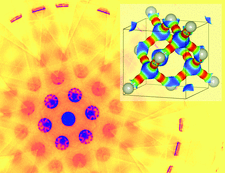
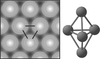
Cover illustration: Electron-density isosurface of silicon coloured with electrostatic potential (red for lowest and blue for highest), together with a convergent-beam electron-diffraction (CBED) pattern of silicon. The red regions between neighbouring atoms indicate that the electrostatic potential is lowered due to the excess (bonding) electrons. The electrostatic potential and electron density were determined using a CBED structure-refinement method [Ogata et al. (2008), Acta Cryst. A64, 587-597]. The figure was drawn using VESTA [Momma & Izumi (2008), J. Appl. Cryst. 41, 653-658].
lead articles


Free 
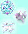
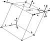
Systematic enumeration of tilings of the two-dimensional hyperbolic plane leads to ab initio construction of triply periodic nets via projection of the tilings onto triply periodic minimal surfaces. The technique is described in detail for kaleidoscopic tilings, projected onto the P, D and G (gyroid) minimal surfaces.
research papers
A general approach for determining the diffraction contrast factor of straight-line dislocations in elastically anisotropic crystals and polycrystals is described. The new approach is illustrated with practical examples of hexagonal metals and some low-symmetry mineral phases.
The use of symmetry as an additional constraint in the charge-flipping algorithm is investigated.
A more accurate method of calculating a molecular shape function from measured small-angle X-ray scattering over a potentially wider range of the magnitude of the momentum transfer is proposed.
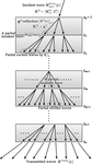
A new many-beam dynamical theory for plan-view high-resolution transmission electron microscopy images of multilayer systems without the limitation of a superlattice cell is proposed. Simulations using this method revealed that characteristic moiré-like lattice fringes are formed due to the relative shift of the crystal-lattice planes.
The topologies of the charge densities in the hexagonal close-packed metals Ru and Zr are shown to be different.
It is shown how the diagrams of symmetry elements given by Litvin [Acta Cryst. (2008), A64, 419–424 and supplementary material] can be interpreted in terms of Belov–Neronova–Smirnova symbols instead of the Opechowski–Guccione symbols favoured by Litvin.
Generating functions are given for the number of nonequivalent sublattices of a parent lattice of given plane symmetry.
book reviews
Free