journal menu


issue contents
September 2009 issue

Cover illustration: Electron-density isosurface of silicon coloured with electrostatic potential (red for lowest and blue for highest), together with a convergent-beam electron-diffraction (CBED) pattern of silicon. The red regions between neighbouring atoms indicate that the electrostatic potential is lowered due to the excess (bonding) electrons. The electrostatic potential and electron density were determined using a CBED structure-refinement method [Ogata et al. (2008), Acta Cryst. A64, 587-597]. The figure was drawn using VESTA [Momma & Izumi (2008), J. Appl. Cryst. 41, 653-658].
research papers


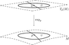
Using differential geometry, a unified description of the symmetry of crystals is presented. This formalism does not require additional dimensions in the modulated case, for which the modulation wave is expressed by a particular parameterization of three-dimensional space.
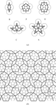
A general construction principle for the inflation rules for decagonal quasiperiodic tilings is proposed.
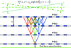
The concept of interbranch phase modulation of an X-ray wavefield is extended to the case of a large gradient, which depends on the depth inside the crystal. Diffraction (extinction) contrast is also discussed for a strongly deformed specimen containing a single dislocation.
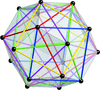
Properties of periodic edge-transitive nets with one vertex in the primitive unit cell are described.
The use of dynamically scattered electrons for three-dimensional potential reconstruction is described.


Louis Pasteur's crystallographic and chemical work is described.
international union of crystallography
Free