journal menu


issue contents
May 2009 issue
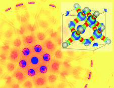
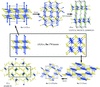
Cover illustration: Electron-density isosurface of silicon coloured with electrostatic potential (red for lowest and blue for highest), together with a convergent-beam electron-diffraction (CBED) pattern of silicon. The red regions between neighbouring atoms indicate that the electrostatic potential is lowered due to the excess (bonding) electrons. The electrostatic potential and electron density were determined using a CBED structure-refinement method [Ogata et al. (2008), Acta Cryst. A64, 587-597]. The figure was drawn using VESTA [Momma & Izumi (2008), J. Appl. Cryst. 41, 653-658].
feature articles


Free 
The birth and growth of the publications and journals of the International Union of Crystallography from 1948 to 2008 are described. Details are given of the pre-war history that led up to their creation and development.
research papers
Atomic scattering factors are modified to correct the resolution bias in electron-density maps.
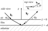
A procedure for obtaining depth-specific scattering profiles of laterally defined nanostructure using grazing-incidence small-angle X-ray scattering is described.

The TOPOS program package was used to generate all subnets of 3- to 12-coordinated binodal nets taken from the Reticular Chemistry Structure Resource database. 38 304 binodal nets with novel topologies were revealed and stored in the TTD collection.

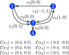
On the basis of a link between a graph-theoretical description of crystal structures and their symmetries, atom positions are constrained. Examples show the presence of implicit and forbidden symmetries.
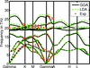
The Debye–Waller factors of wurtzite-type semiconductors are calculated from ab initio force constants and fitted in the temperature range from 0.1 to 1000 K.
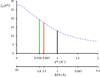
The exact relationship between the atomic pair distribution function and small-angle-scattering equations is established and discussed. This has implications for the structural modeling of nanoparticles.
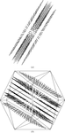
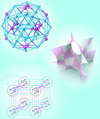
The main problems in the discrete tomography of mathematical quasicrystals with icosahedral symmetry are investigated.

The full symmetry groups of carbon nanotori are investigated and the irreducible representations and characters of the symmetry groups of chiral and achiral nanotori are discussed.